| CPC H10K 59/353 (2023.02) [G09G 3/20 (2013.01); G09G 3/3225 (2013.01); H10K 59/12 (2023.02); H10K 59/122 (2023.02); G09G 2300/0452 (2013.01); G09G 2310/0264 (2013.01); G09G 2310/0291 (2013.01); G09G 2354/00 (2013.01); H10K 50/11 (2023.02); H10K 50/15 (2023.02); H10K 50/16 (2023.02); H10K 50/17 (2023.02); H10K 50/81 (2023.02); H10K 50/82 (2023.02); H10K 59/352 (2023.02)] | 16 Claims |
|
[ 17. An organic light-emitting display device comprising:
a substrate including a plurality of pixels, the plurality of pixels comprising a first sub-pixel, a second sub-pixel and a third sub-pixel, each of the first to third sub-pixels having an emission portion and a non-emission portion surrounding the emission portion;
a first electrode on the emission portion of each of the first to third sub-pixels;
a bank on the non-emission portion;
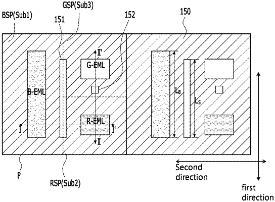
a first spacer between the emission portion of the first sub-pixel and the emission portion of the second sub-pixel to block the emission portion of the second sub-pixel from the emission portion of the first sub-pixel;
a second spacer placed between the second sub-pixel and the third sub-pixel, wherein the second spacer is higher in height in a vertical direction from the bank than the first spacer;
an organic stack above the first electrode and the first spacer, wherein the organic stack has at least a first organic stack, a second organic stack, and a charge generation layer, the first organic stack disposed on the first electrode and the first spacer, the second organic stack disposed on the first organic stack, and the charge generation layer disposed between the first and second organic stacks; and
a second electrode on the organic stack. ]
|