US D1,064,005 S
Grounding ring of a process kit for semiconductor substrate processing
Abhishek Chowdhury, Bangalore (IN); Nataraj Bhaskar Rao, Bangalore (IN); Edwin C. Suarez, Pleasanton, CA (US); Harisha Sathyanarayana, Bangalore (IN); Diego Ramiro Puente Sotomayor, Phoenix, AZ (US); Qanit Takmeel, Mesa, AZ (US); Mohammad Kamruzzaman Chowdhury, Phoenix, AZ (US); and Arun Chakravarthy Chakravarthy, Tamil Nadu (IN)
Assigned to APPLIED MATERIALS, INC., Santa Clara, CA (US)
Filed by Applied Materials, Inc., Santa Clara, CA (US)
Filed on Aug. 4, 2022, as Appl. No. 29/848,745.
Term of patent 15 Years
LOC (15) Cl. 13 - 03
U.S. Cl. D15—138  [D13/182]
OG exemplary drawing
 
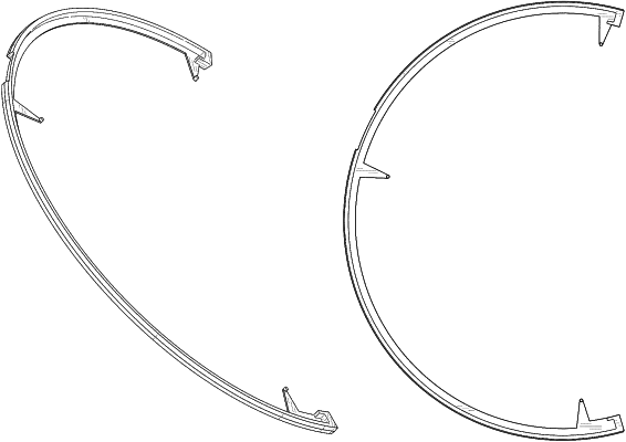
The ornamental design for a grounding ring of a process kit for semiconductor substrate processing, as shown and described.