| CPC H10N 50/80 (2023.02) [H10B 61/00 (2023.02); H10N 50/01 (2023.02)] | 20 Claims |
|
1. An embedded device, comprising:
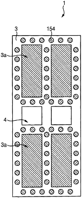
a substrate including a magnetic random access memory (MRAM) region, the MRAM region having a cell block region;
magnetic tunnel junction (MTJ) modules in the cell block region, each of the MTJ modules including a MTJ pattern;
an insulating interlayer structure covering the MTJ modules; and
a plurality of magnetic field shielding structures in the insulating interlayer structure and adjacent to an outside of the cell block region,
wherein
each of the magnetic field shielding structures extends in a vertical direction from an upper end of the MTJ pattern to a lower end of the MTJ pattern,
each of the magnetic field shielding structures includes a ferromagnetic material, and
each of the magnetic field shielding structures has a sidewall inclined at an oblique angle with respect to the substrate.
|