| CPC H10K 59/40 (2023.02) [G06F 3/0445 (2019.05); G06F 3/0446 (2019.05); H10K 50/86 (2023.02); G06F 2203/04111 (2013.01); G06F 2203/04112 (2013.01); H01L 27/124 (2013.01); H10K 59/1213 (2023.02)] | 22 Claims |
|
1. A display device comprising:
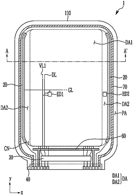
a display area that includes a first display area and a second display area adjacent to each other;
a gate driver that includes a driving circuit, at least part of the driving circuit being disposed in the second display area;
first pixel circuit units disposed in the first display area;
first light emitting elements disposed in the first display area and electrically connected to the first pixel circuit units;
second pixel circuit units disposed in the second display area;
second light emitting elements disposed in the second display area and two or more of the second light emitting elements are electrically connected to one of the second pixel circuit units; and
a light blocking layer overlapping at least one of the second light emitting elements in a plan view.
|