| CPC H10K 59/40 (2023.02) [G06F 3/0412 (2013.01); G06F 3/0445 (2019.05); G06F 3/0446 (2019.05); H10K 71/00 (2023.02); G06F 2203/04103 (2013.01); G06F 2203/04111 (2013.01); H10K 59/1201 (2023.02); H10K 59/131 (2023.02)] | 14 Claims |
|
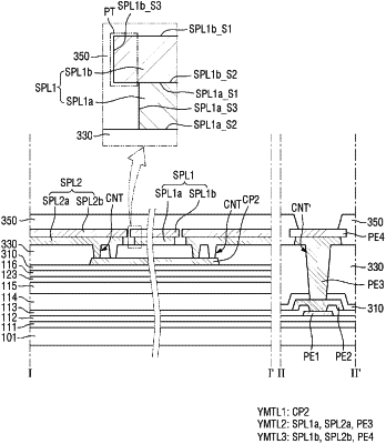
1. A display device comprising:
a display member; and
a touch member which is disposed on the display member,
wherein the touch member comprises:
a first touch insulating layer which is disposed on the display member;
a first touch conductive layer which is disposed on the first touch insulating layer and comprises a touch bridge electrode;
a second touch insulating layer which is disposed on the first touch conductive layer, comprises an organic material, and comprises a first contact hole penetrating the second touch insulating layer in a thickness direction;
a second touch conductive layer which is disposed on the second touch insulating layer and comprises a first lower sensing line overlapping the touch bridge electrode; and
a third touch conductive layer which is disposed on the second touch conductive layer and comprises a first upper sensing line overlapping the first lower sensing line,
wherein a width of the first upper sensing line is greater than a width of the first lower sensing line.
|