| CPC H10K 59/131 (2023.02) [G09G 3/3233 (2013.01); H10K 59/1213 (2023.02); H10K 59/1216 (2023.02); H10K 77/111 (2023.02); G09G 2300/0861 (2013.01); G09G 2310/0251 (2013.01); G09G 2310/0262 (2013.01); G09G 2320/043 (2013.01); H01L 27/124 (2013.01); H01L 27/1255 (2013.01); H01L 28/60 (2013.01); H01L 29/45 (2013.01); H01L 29/4908 (2013.01); H10K 50/80 (2023.02); H10K 2102/311 (2023.02); Y02E 10/549 (2013.01)] | 13 Claims |
|
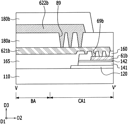
1. A display device, comprising:
a substrate including a bending area and a first contact area disposed at a first side of the bending area; and
a first wire disposed on the substrate and including:
a first conductive part disposed in the first contact area,
a second conductive part overlapping the first conductive part and disposed in at least the first contact area and the bending area, and
a third conductive part overlapping the second conductive part and disposed in at least the first contact area,
wherein the second conductive part is directly connected to the first conductive part in the first contact area, and the third conductive part is directly connected to the second conductive part in the first contact area, and
wherein the second conductive part and the third conductive part are not connected to each other in the bending area.
|