| CPC H10K 59/131 (2023.02) [G09G 3/3233 (2013.01); H10K 59/12 (2023.02); H10K 59/1216 (2023.02); H10K 59/1315 (2023.02)] | 17 Claims |
|
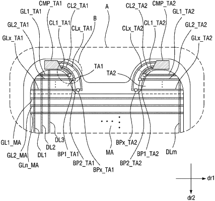
1. A light-emitting display device comprising:
a substrate on which a display area and a non-display area are defined, wherein the display area comprises a first area and a second area, and a plurality of pixels is in the display area;
a first signal line on the substrate in the first area;
a second signal line on the substrate in the second area;
a compensation line on the substrate in the non-display area;
a bridge pattern over the second signal line and the compensation line in the non-display area and electrically connecting the second signal line with the compensation line;
a first insulating layer between the bridge pattern and the compensation line, the first insulating layer including a first surface facing the substrate and a second surface opposite to the first surface; and
a compensation metal pattern over the compensation line in the non-display area and overlapping with the compensation line,
wherein the bridge pattern comprises a first bridge metal pattern, a second bridge metal pattern, and a third bridge metal pattern,
wherein the first bridge metal pattern is over the second signal line and electrically connected to the second signal line,
wherein the second bridge metal pattern is over the compensation line and electrically connected to the compensation line,
wherein the third bridge metal pattern is over the first bridge metal pattern and the second bridge metal pattern and electrically connects the first bridge metal pattern with the second bridge metal pattern, and
wherein the first bridge metal pattern, the second bridge metal pattern, and the compensation metal pattern directly contact the second surface of the first insulating layer.
|