| CPC H10K 59/131 (2023.02) [G09G 3/3258 (2013.01); G09G 3/3266 (2013.01); G09G 3/3291 (2013.01); H01L 27/124 (2013.01); H01L 27/1248 (2013.01); H10K 50/8445 (2023.02); H10K 59/124 (2023.02); H10K 77/111 (2023.02); G09G 2300/0426 (2013.01); H10K 2102/311 (2023.02)] | 13 Claims |
|
1. A display device, comprising:
a substrate comprising a display area and a peripheral area disposed outside of the display area;
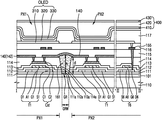
a plurality of display elements and a plurality of pixel-circuits on the display area, the plurality of pixel-circuits includes a first pixel-circuit and a second pixel-circuit disposed adjacent to each other in a first direction;
an inorganic insulating layer disposed in the display area, wherein the inorganic insulating layer comprises a groove disposed in a region between the first pixel-circuit and the second pixel-circuit; and
a first vertical connection wiring disposed over the inorganic insulating layer and extending in the first direction across the groove,
wherein a semiconductor layer of the first pixel-circuit is spaced apart from a semiconductor layer of the second pixel-circuit by the groove, and the semiconductor layer of the first pixel-circuit is connected to the semiconductor layer of the second pixel-circuit by the first vertical connection wiring,
wherein the groove surrounds at least some of the plurality of pixel-circuits.
|