| CPC H10K 59/131 (2023.02) [H10K 59/1201 (2023.02)] | 20 Claims |
|
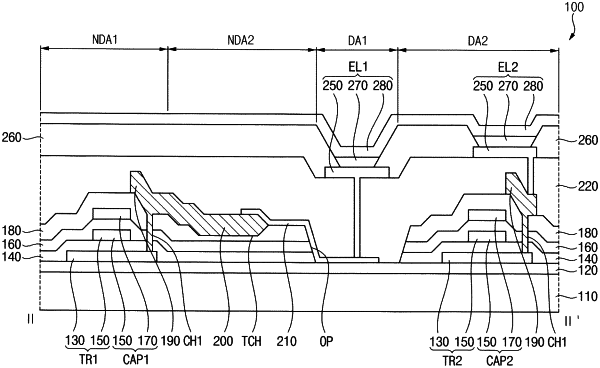
1. A display device, comprising:
a substrate including a first display area, a first non-display area spaced apart from the first display area, and a second non-display area disposed between the first display area and the first non-display area;
a first light emitting element disposed on the substrate in the first display area;
a first pixel circuit disposed on the substrate in the first non-display area and electrically connected to the first light emitting element;
a first insulating layer disposed on the substrate, covering the first pixel circuit, and including a first surface facing the substrate;
a metal wiring disposed on the first insulating layer, connected to the first pixel circuit, extending from the first non-display area to the second non-display area, and including a first surface facing the first insulating layer; and
a transparent wiring disposed on the first insulating layer, connecting the first light emitting element and the metal wiring, and extending from the first display area to a second surface of the metal wiring opposite to the first surface of the metal wiring,
wherein a trench is defined in a second surface of the first insulating layer opposite to the first surface of the first insulating layer in the second non-display area, and
wherein the metal wiring is disposed in the trench in the second non-display area.
|