| CPC H10K 59/131 (2023.02) [H10K 50/865 (2023.02); H10K 59/60 (2023.02)] | 21 Claims |
|
1. A display device, comprising:
a substrate including a display area having a plurality of pixel areas and a non-display area surrounding at least one side of the display area;
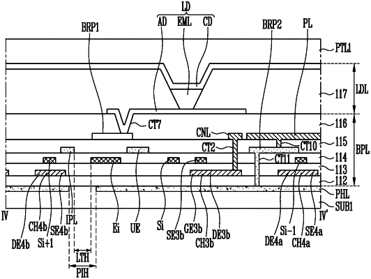
a light-blocking layer disposed on a first surface of the substrate and comprising a single layer having light transmissive areas disposed across substantially the entire width of the display area to allow incident light to pass therethrough;
a circuit-element layer disposed on the light-blocking layer and comprising a plurality of conductive layers, at least one first contact hole, and a semiconductor layer in the display area;
a light-emitting element layer disposed on the circuit-element layer and including light-emitting elements; and
a sensor layer disposed on a second surface of the substrate opposing the first surface and extending across substantially the entire width of the display area to sense the light passing through the light transmissive areas,
wherein the light-blocking layer is electrically coupled to at least one of the plurality of conductive layers through the at least one first contact hole disposed in the display area, and the light-blocking layer is disposed between the semiconductor layer and the sensor layer, and
wherein the at least one of the plurality of conductive layers electrically coupled to the light-blocking layer is disposed between the light-emitting element layer and the semiconductor layer.
|