| CPC H10K 59/126 (2023.02) [H10K 71/00 (2023.02); H10K 59/1201 (2023.02)] | 12 Claims |
|
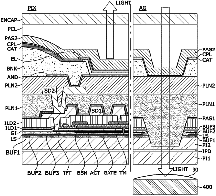
1. A method of fabricating a display panel including a display region including a first pixel region where a plurality of pixels are disposed, a sensing region including a second pixel region where a plurality of pixel groups are disposed and a light transmitting part disposed between the pixel groups, and a circuit layer including a plurality of transistors disposed in the first and second pixel regions, the method comprising:
forming a light shield layer at least in the sensing region, wherein the light shield layer in the sensing region includes a first hole corresponding to the light transmitting part;
forming a metal layer spaced apart from the light blocking shield layer in the display region and the sensing region; and
irradiating a laser beam to at least the sensing region to remove the metal layer from the light transmitting part so the metal layer in the sensing region includes a second hole that overlaps with the first hole in the light shield layer.
|