| CPC H10K 59/124 (2023.02) [H10K 50/844 (2023.02); H10K 59/40 (2023.02); G06F 3/0412 (2013.01); H10K 50/868 (2023.02); H10K 59/1213 (2023.02); H10K 59/1216 (2023.02); H10K 59/122 (2023.02); H10K 59/123 (2023.02); H10K 59/126 (2023.02); H10K 59/131 (2023.02); H10K 59/352 (2023.02); H10K 59/38 (2023.02); H10K 2102/351 (2023.02)] | 20 Claims |
|
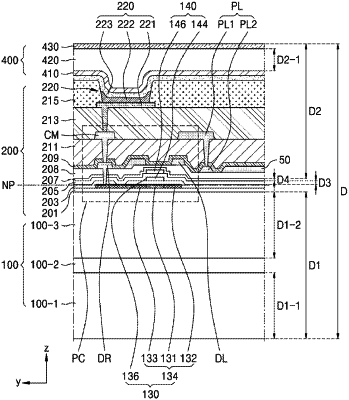
1. A display device comprising:
a substrate;
a semiconductor layer on the substrate;
a first interlayer insulating layer on the semiconductor layer;
a second interlayer insulating layer on the first interlayer insulating layer;
a source electrode or a drain electrode on the second interlayer insulating layer, and connected to the semiconductor layer;
an organic light-emitting diode connected to the source electrode or the drain electrode; and
a thin film encapsulation layer on the organic light-emitting diode,
wherein, a neutral plane is inside or below the first interlayer insulating layer or the second interlayer insulating layer, such that a compressive force on one side of the neutral plane corresponding to an impact applied to the thin film encapsulation layer causes a tensile force on another side of the neutral plane.
|