| CPC H10K 59/124 (2023.02) [H10K 59/131 (2023.02)] | 19 Claims |
|
1. A display apparatus comprising:
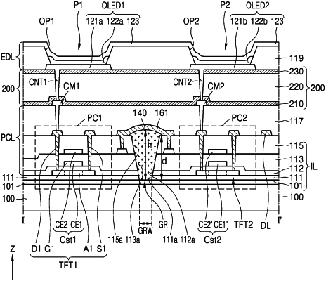
a substrate having a display area;
a plurality of pixel circuits arranged in the display area, each of the pixel circuits including a thin-film transistor, the thin-film transistor including a semiconductor layer, a source electrode on the semiconductor layer, a drain electrode on the semiconductor layer, and a gate electrode on the semiconductor layer;
a planarization layer comprising an organic material and covering the thin-film transistor, a top surface of the planarization layer being flat;
a connection electrode directly disposed on the planarization layer, the connection electrode being directly connected to one of the source electrode or the drain electrode of the thin-film-transistor;
a composite layer disposed on the connection electrode, the composite layer comprising a first inorganic insulating layer overlapping at least a semiconductor layer of one thin-film transistor, a first organic insulating layer overlapping the at least the semiconductor layer of the one thin-film transistor, and a second inorganic insulating layer overlapping the at least the semiconductor layer of the one thin-film transistor, the first inorganic insulating layer, the first organic layer, and the second inorganic insulating layer being sequentially stacked; and
a plurality of display elements disposed on and above the composite layer, the plurality of display elements respectively connected to the pixel circuits with each display element including a pixel electrode and an emission layer on and directly over the pixel electrode,
wherein the first inorganic insulating layer is directly disposed on the connection electrode and the planarization layer,
the first inorganic insulating layer is thinner than the planarization layer.
|