| CPC H10K 59/122 (2023.02) [H10K 59/1201 (2023.02); H10K 59/80522 (2023.02)] | 19 Claims |
|
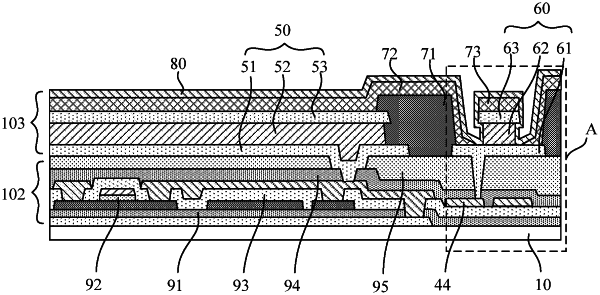
1. A display substrate, comprising a driving circuit layer arranged on a base and a light emitting structure layer arranged on one side, away from the base, of the driving circuit layer, wherein the light emitting structure layer comprises an anode, a pixel definition layer, an organic light emitting layer, a cathode, and an auxiliary electrode;
the pixel definition layer has a first pixel opening exposing the anode and a second pixel opening exposing the auxiliary electrode; the organic light emitting layer connected to the anode and the cathode connected to the organic light emitting layer are arranged in the first pixel opening; the organic light emitting layer separated from the auxiliary electrode and the cathode located on one side, away from the base, of the organic light emitting layer are arranged in the second pixel opening; and the cathode is connected to the auxiliary electrode in the second pixel opening,
wherein the auxiliary electrode comprises a first auxiliary electrode, a second auxiliary electrode arranged on one side, away from the base, of the first auxiliary electrode, and a third auxiliary electrode arranged on one side, away from the base, of the second auxiliary electrode; an orthographic projection of the second auxiliary electrode on the base is located within a range of an orthographic projection of the third auxiliary electrode on the base; and the orthographic projection of the second auxiliary electrode on the base is located within a range of an orthographic projection of the first auxiliary electrode on the base.
|