| CPC H10K 59/1213 (2023.02) [G09G 3/3233 (2013.01); H10K 59/1216 (2023.02); H10K 59/131 (2023.02); G09G 2300/0819 (2013.01); G09G 2300/0852 (2013.01); G09G 2300/0861 (2013.01); G09G 2320/0209 (2013.01); G09G 2320/0219 (2013.01); H01L 27/1225 (2013.01); H01L 27/124 (2013.01); H01L 27/1251 (2013.01); H01L 27/1255 (2013.01); H01L 29/78675 (2013.01); H01L 29/7869 (2013.01)] | 13 Claims |
|
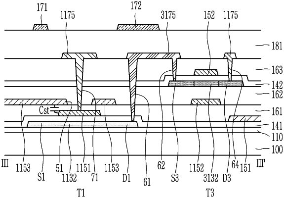
1. An emissive display device comprising:
a plurality of data lines extending in a first direction;
a first semiconductor including a channel, a source region, and a drain region of a driving transistor disposed on a substrate;
a gate electrode of the driving transistor overlapping the channel of the driving transistor;
a second semiconductor including a channel, a source region, and a drain region of a second transistor disposed on the substrate;
a first connection electrode including:
a first connector electrically connected to the gate electrode of the driving transistor;
a first electrode of the second transistor;
a second connector electrically connected to a second electrode of the second transistor; and
a main body disposed between the first connector and the second connector; and
a voltage line disposed on the substrate and applying a first voltage having a constant level of voltage,
wherein the voltage line surrounds at least a part of the second connector of the first connection electrode, and
the part of the second connector of the first connection electrode surrounded by the voltage line is disposed between adjacent two of the plurality of data lines in a plan view.
|