| CPC H10K 59/121 (2023.02) [H10K 50/844 (2023.02); H10K 59/131 (2023.02); H10K 59/40 (2023.02); H10K 59/65 (2023.02); H10K 71/00 (2023.02); H10K 77/10 (2023.02); H10K 59/1201 (2023.02)] | 10 Claims |
|
1. A method of manufacturing a display device, the method comprising:
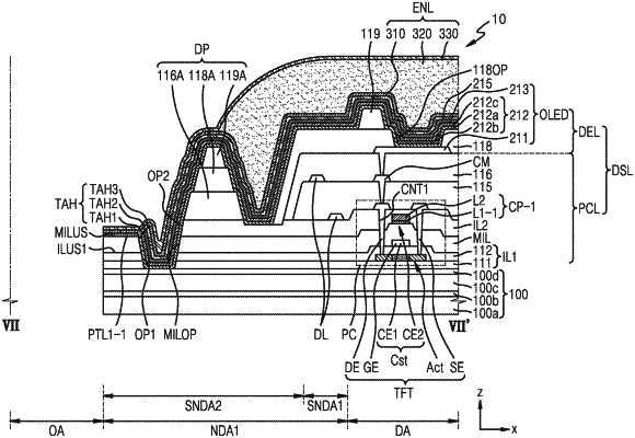
preparing a display substrate comprising a substrate and a first insulating layer on the substrate, the substrate comprising a non-display area and a display area;
forming, on the first insulating layer, a conductive pattern comprising a first layer and a second layer;
forming, in the non-display area, a pattern layer comprising a lower pattern layer and an upper pattern layer;
forming a conductive layer on the pattern layer and the display area;
patterning the conductive layer to form a first electrode; and
removing the upper pattern layer,
wherein the lower pattern layer and the first layer include a same material, and
wherein the upper pattern layer and the second layer include a same material.
|