| CPC H10K 50/844 (2023.02) [H10K 59/122 (2023.02)] | 15 Claims |

|
1. A display apparatus comprising:
a substrate including a display area and a peripheral area adjacent to the display area;
a thin film transistor arranged in the display area and including a semiconductor layer, a gate electrode, a source electrode, and a drain electrode;
a first inorganic insulating layer located on the substrate and under the gate electrode and covering the semiconductor layer;
a second inorganic insulating layer located on the first inorganic insulating layer and covering the gate electrode;
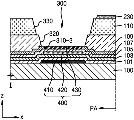
a third inorganic insulating layer located on the second inorganic insulating layer and including a third inorganic insulating layer opening in the peripheral area;
an organic insulating layer located on the third inorganic insulating layer, covering the source electrode and the drain electrode, and including a second opening overlapping the third inorganic insulating layer opening in the peripheral area; and
a pattern portion located on a layer under the organic insulating layer and overlapping the third inorganic insulating layer opening and the second opening, wherein
the third inorganic insulating layer opening is not filled with an organic material,
the pattern portion overlaps the first inorganic insulating layer and/or the second inorganic insulating layer between the substrate and the third inorganic insulating layer opening of the third inorganic insulating layer, and
respective portions of the first inorganic insulating layer and/or the second inorganic insulating layer overlapping the patterned portion have an overlapping portion including a top surface elevated above a top surface of a non-overlapping portion by a height as high as a height of the pattern portion.
|