| CPC H10K 50/824 (2023.02) [H10K 59/123 (2023.02); H10K 59/124 (2023.02); H10K 50/15 (2023.02); H10K 50/16 (2023.02); H10K 50/17 (2023.02); H10K 50/171 (2023.02); H10K 50/19 (2023.02); H10K 50/828 (2023.02); H10K 2102/3026 (2023.02)] | 23 Claims |
|
1. A display device, comprising:
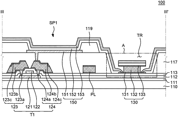
a substrate including a plurality of sub-pixels;
a transistor disposed on the substrate and including a gate electrode, an active layer, a source electrode and a drain electrode;
at least one planarization layer covering the source and drain electrodes of the transistor, and including a trench formed therethrough adjacent to the plurality of sub-pixels;
a plurality of light emitting elements disposed in the plurality of sub-pixels and sharing an organic layer and a cathode disposed on the organic laver;
an auxiliary electrode disposed in the trench and connected to the cathode; and
a bank disposed on the at least one planarization layer, and defining and separating the plurality of sub-pixels and the auxiliary electrode,
wherein a side surface of the auxiliary electrode has a concave shape,
wherein the organic layer has an open portion that is disconnected by the concave shape of the auxiliary electrode,
wherein the auxiliary electrode includes a first layer including titanium Ti, a second layer disposed on the first electrode and including aluminum Al, and a third layer disposed on the second layer and including titanium Ti,
wherein the at least one planarization layer includes a lower planarization layer covering the transistor and an upper planarization layer on the lower planarization layer,
wherein the auxiliary electrode is disposed on the lower planarization layer, and
wherein the lower planarization layer includes a groove exposing a portion of a bottom surface of the first layer.
|