US 12,238,948 B2
Imaging element, stacked imaging element, and solid-state imaging device
Toshiki Moriwaki, Tokyo (JP)
Assigned to SONY GROUP CORPORATION, Tokyo (JP)
Filed by SONY GROUP CORPORATION, Tokyo (JP)
Filed on Oct. 9, 2023, as Appl. No. 18/483,162.
Application 18/483,162 is a continuation of application No. 17/250,717, granted, now 11,800,729, previously published as PCT/JP2019/034146, filed on Aug. 30, 2019.
Claims priority of application No. 2018-165081 (JP), filed on Sep. 4, 2018.
Prior Publication US 2024/0057362 A1, Feb. 15, 2024
This patent is subject to a terminal disclaimer.
Int. Cl. H10K 39/32 (2023.01); H10K 30/30 (2023.01)
CPC H10K 39/32 (2023.02) [H10K 30/30 (2023.02)] 14 Claims
OG exemplary drawing
 
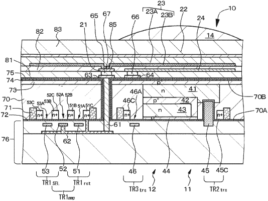
1. A light detecting element, comprising:
a first electrode;
a second electrode;
a photoelectric conversion layer between the first electrode and the second electrode; and
an inorganic oxide semiconductor material layer between the first electrode and the photoelectric conversion layer, wherein the inorganic oxide semiconductor material layer contains indium atoms, tin atoms, titanium atoms, and zinc atoms.