| CPC H10K 39/32 (2023.02) [A61B 1/05 (2013.01)] | 12 Claims |
|
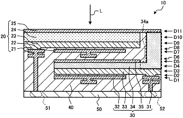
1. A solid-state imaging device, comprising:
a first photoelectric conversion portion that includes:
a first electrode;
a first photoelectric conversion layer electrically connected to the first electrode; and
a second electrode on a first surface of the first photoelectric conversion layer, wherein
the second electrode is on a light incidence side of the first photoelectric conversion portion, and
the first photoelectric conversion layer has a protrusion region; and
a second photoelectric conversion portion on the light incidence side of the first photoelectric conversion portion, wherein
the second photoelectric conversion portion includes a third electrode, and
the protrusion region of the first photoelectric conversion layer protrudes from a portion of the first photoelectric conversion layer and reaches to the third electrode.
|