| CPC H10F 71/125 (2025.01) [H10F 10/13 (2025.01); H10F 10/162 (2025.01); H10F 71/1253 (2025.01); H10F 77/1237 (2025.01); H10F 77/211 (2025.01); Y02E 10/543 (2013.01); Y02P 70/50 (2015.11)] | 20 Claims |
|
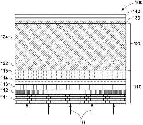
1. A photovoltaic device, comprising:
a layer stack;
a back contact layer; and
an absorber layer disposed between the layer stack and the back contact layer, the absorber layer comprising a front interface and a back interface; wherein:
the absorber layer is an alloy comprising cadmium, tellurium, and selenium;
the absorber layer includes a varying concentration of selenium such that there is a higher concentration of selenium near the front interface relative to the back interface;
an atomic concentration of selenium varies non-linearly across a thickness of the absorber layer;
the absorber layer comprises a first region and a second region, the first region disposed proximate to the layer stack relative to the second region;
the first region has a thickness between 100 nanometers to 3000 nanometers;
the second region has a thickness between 100 nanometers to 3000 nanometers;
an average atomic concentration of selenium in the first region is greater than an average atomic concentration of selenium in the second region; and
a ratio of an average atomic concentration of selenium in the first region to an average atomic concentration of selenium in the second region is greater than 2.
|