| CPC H10D 84/834 (2025.01) [H01L 21/3086 (2013.01); H10D 30/024 (2025.01); H10D 30/6211 (2025.01); H10D 64/017 (2025.01); H10D 64/018 (2025.01); H10D 64/021 (2025.01); H10D 84/0135 (2025.01); H10D 84/0147 (2025.01); H10D 84/0151 (2025.01); H10D 84/0158 (2025.01); H10D 84/038 (2025.01)] | 20 Claims |
|
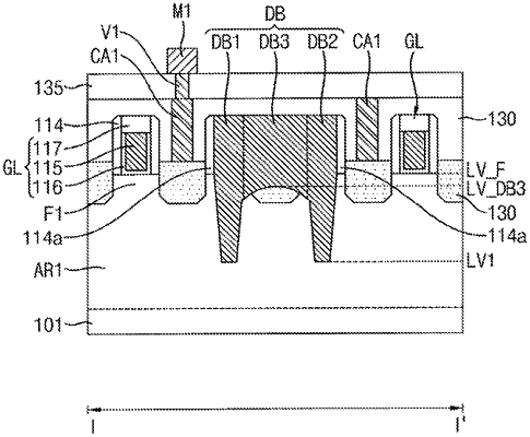
1. A semiconductor device, comprising:
a substrate having a first region and a second region;
first active fins that extend in a first direction in the first region;
second active fins that extend in the first direction in the second region;
a first field insulating layer between the first active fins and extending in a second direction;
a second field insulating layer between the second active fins and extending in the second direction;
a gate line that extends in the second direction on the second field insulating layer; and
a gate isolation layer in contact with a side surface of the first field insulating layer in the second direction,
wherein an upper surface of the first field insulating layer is at a first level and an upper surface of the second field insulating layer is at a second level that is lower than the first level, and
wherein a bottom surface of the first field insulating layer is at a third level and a bottom surface of the second field insulating layer is at a fourth level that is different from the third level.
|