| CPC H10B 53/40 (2023.02) | 20 Claims |
|
1. An apparatus comprising:
a first pedestal;
a second pedestal;
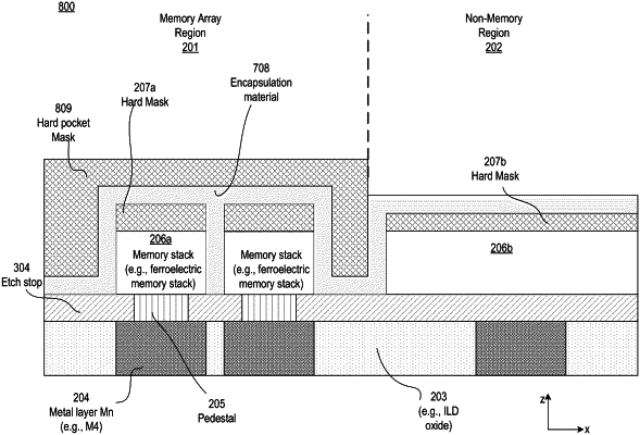
an etch stop layer, wherein the first pedestal is separated by the second pedestal by the etch stop layer;
a first memory device comprising a first stack of materials, wherein a first portion of the first stack of materials is on the first pedestal;
a second memory device comprising a second stack of materials, wherein a second portion of the second stack of materials is on the second pedestal;
a first hard mask layer on the first memory device;
a second hard mask layer on the first memory device, wherein the first hard mask layer and the second hard mask layer are separated by a first metal via;
a first protection layer on the first hard mask layer;
a second protection layer on the second hard mask layer, wherein the first protection layer and the second protection layer are separated by the first metal via;
a third hard mask layer on the second memory device;
a fourth hard mask layer on the second memory device, wherein the third hard mask layer and the fourth hard mask layer are separated by a second metal via;
a third protection layer on the third hard mask layer;
a fourth protection layer on the fourth hard mask layer, wherein the third protection layer and the fourth protection layer are separated by the second metal via; and
an encapsulation material between the first memory device, the second memory device, the second hard mask layer, the second protection layer; the third hard mask layer, and the third protection layer, wherein the encapsulation material is on the etch stop layer and separates an interlayer dielectric from the etch stop layer.
|