| CPC H10B 53/00 (2023.02) [H01L 28/40 (2013.01)] | 20 Claims |
|
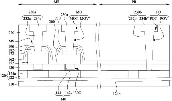
1. A method for fabricating a semiconductor device, comprising:
depositing a ferroelectric layer over a substrate;
performing a first ionized physical deposition process to deposit a top electrode layer over and in contact with the ferroelectric layer, wherein the first ionized physical deposition process is performed with an AC bias in a range from about 0 W to about 50 W, and the AC bias does not exceed 50 W to prevent a ratio of non-ferro phase in the ferroelectric layer from increasing, wherein the ferroelectric layer is exposed to ionized metal atoms during the first ionized physical deposition process;
patterning the top electrode layer into a top electrode; and
patterning the ferroelectric layer into a ferroelectric element below the top electrode.
|