| CPC H10B 43/40 (2023.02) [H10B 41/27 (2023.02); H10B 41/41 (2023.02); H10B 43/27 (2023.02)] | 20 Claims |
|
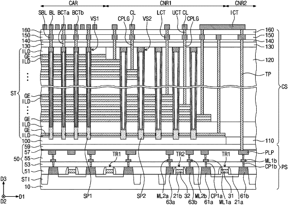
1. A semiconductor device, comprising:
a gate electrode on a semiconductor substrate;
a gate insulating layer between the gate electrode and the semiconductor substrate;
an interlayer insulating layer on the semiconductor substrate to cover the gate electrode;
a first epitaxial layer disposed on the semiconductor substrate and at a first side of the gate electrode;
a second epitaxial layer disposed on the semiconductor substrate and at a second side, opposite to the first side, of the gate electrode;
a first contact plug in contact with a first portion of the first epitaxial layer; and
a second contact plug in contact with a first portion of the second epitaxial layer,
wherein a top surfaces of the first epitaxial layer and a top surface of the second epitaxial layer are located at a level higher than a top surface of the gate electrode, and
wherein the interlayer insulating layer has a top surface located at substantially the same level as the top surfaces of the first and second epitaxial layers.
|