| CPC H10B 41/27 (2023.02) [H10B 12/0335 (2023.02); H10B 10/18 (2023.02)] | 9 Claims |
|
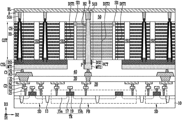
1. A semiconductor memory device comprising:
a common source line;
a bit line spaced apart from the common source line in a vertical direction;
a gate stack structure including interlayer insulating layers and conductive patterns, and including a hole, wherein the interlayer insulating layers and the conductive patterns are alternately stacked between the common source line and the bit line, and wherein the hole has a tapered shape that becomes narrower near the bit line and wider near the common source line;
a memory layer formed along the hole; and
a channel structure disposed on the memory layer, the channel structure being connected to the common source line and the bit line.
|