US 12,238,925 B2
Semiconductor memory device capable of expanding bank capacity adaptively to package size and method of designing the same
Ik-Joon Choi, Suwon-si (KR); Kihyun Kim, Suwon-si (KR); Sungchul Park, Suwon-si (KR); Minjun Kim, Suwon-si (KR); and Junhyung Kim, Suwon-si (KR)
Assigned to Samsung Electronics Co., Ltd., (KR)
Filed by Samsung Electronics Co., Ltd., Suwon-si (KR)
Filed on May 5, 2023, as Appl. No. 18/143,756.
Claims priority of application No. 10-2022-0100892 (KR), filed on Aug. 11, 2022; and application No. 10-2022-0137303 (KR), filed on Oct. 24, 2022.
Prior Publication US 2024/0057324 A1, Feb. 15, 2024
Int. Cl. H10B 12/00 (2023.01); G11C 11/408 (2006.01)
CPC H10B 12/50 (2023.02) [G11C 11/4087 (2013.01)] 20 Claims
OG exemplary drawing
 
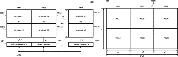
1. A semiconductor memory device comprising n physical banks, each of which is configured to be entirely or partially included in one of a first logic bank or a second logic bank and arranged in a row direction, wherein n is an integer that is greater than or equal to 3, and wherein a proportion of a sum of respective widths of the n physical banks in the row direction to a height of the n physical banks in a column direction is a real number multiple that is not a multiple of 2.