US 12,238,923 B2
Method of forming contact included in semiconductor device
Suncheul Kim, Hwaseong-si (KR); Donghyun Lee, Gwacheon-si (KR); and Uihyoung Lee, Hwaseong-si (KR)
Assigned to Samsung Electronics Co., Ltd., Gyeonggi-do (KR)
Filed by Samsung Electronics Co., Ltd., Suwon-si (KR)
Filed on Nov. 30, 2023, as Appl. No. 18/524,794.
Application 18/524,794 is a continuation of application No. 17/568,117, filed on Jan. 4, 2022, granted, now 11,871,563.
Claims priority of application No. 10-2021-0084676 (KR), filed on Jun. 29, 2021.
Prior Publication US 2024/0098986 A1, Mar. 21, 2024
This patent is subject to a terminal disclaimer.
Int. Cl. H10B 12/00 (2023.01)
CPC H10B 12/485 (2023.02) 10 Claims
OG exemplary drawing
 
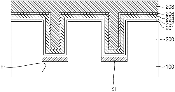
1. A method of forming a contact, the method comprising:
providing a semiconductor substrate comprising a silicon oxide film to an interior of a chamber;
supplying a source gas including TiCl4 and H2 to the interior of the chamber; and
forming a barrier layer by igniting a plasma using the source gas.