| CPC H10B 12/315 (2023.02) [H10B 12/033 (2023.02); H10B 12/34 (2023.02)] | 20 Claims |

|
1. A method for fabricating a semiconductor memory device, the method comprising:
providing a substrate including a first region and a second region, wherein the second region extends along a boundary of the first region;
forming a plurality of word lines in the substrate;
forming a plurality of buried contacts on the substrate;
forming a plurality of landing pads on the plurality of buried contacts, and connected to the buried contacts;
forming a plurality of pre-support patterns between the plurality of landing pads;
forming a plurality of lower electrodes on the plurality of landing pads, and connected to the landing pads;
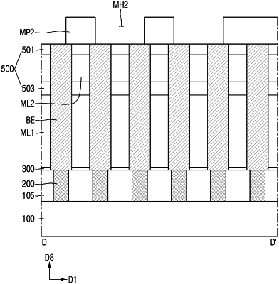
forming a first mask pattern on the first region of the substrate;
removing at least a portion of the plurality of pre-support patterns to form a plurality of support patterns;
forming a capacitive dielectric film on the plurality of lower electrodes; and
forming an upper electrode on the capacitive dielectric film,
wherein the plurality of lower electrodes include a first lower electrode group,
wherein the first lower electrode group comprises six first edge lower electrodes arranged at respective vertices of a hexagonal shape, and one first center lower electrode that is centrally positioned within the hexagonal shape, and
wherein the first mask pattern completely overlaps with the first center lower electrode in a vertical direction perpendicular to an upper surface of the substrate.
|