| CPC H10B 12/315 (2023.02) [H01L 21/764 (2013.01); H01L 21/7682 (2013.01); H01L 29/6656 (2013.01); H10B 12/34 (2023.02); H10B 12/36 (2023.02)] | 20 Claims |
|
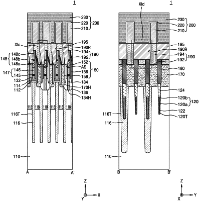
1. A semiconductor device comprising:
a substrate in which a plurality of active regions are defined;
a plurality of bit line structures disposed on the substrate, each of the plurality of bit line structures comprising a bit line and an insulating spacer structure, the insulating spacer structure covering a sidewall of the bit line and having an air spacer, and the bit line structures being spaced apart from each other in a first horizontal direction and extending parallel to each other in a second horizontal direction different from the first horizontal direction;
a plurality of buried contacts and a plurality of insulating fences disposed in lower portions of spaces between the plurality of bit line structures, the plurality of buried contacts and the plurality of insulating fences being alternately arranged in the second horizontal direction;
a plurality of landing pads which fill upper portions of the spaces between the plurality of bit line structures, extend in a vertical direction from upper surfaces of the plurality of buried contacts to upper surfaces of the plurality of bit line structures, and are electrically connected to the plurality of active regions via the plurality of buried contacts;
a plurality of recess portions,
wherein each of the plurality of recess portions extends toward the substrate from between two landing pads, which are spaced apart from each other in the first horizontal direction, among the plurality of landing pads, and
wherein a first recess portion of the plurality of recess portions is defined by a sidewall of a first landing pad of the two landing pads and a first sidewall of a first bit line structure of the plurality of bit line structures; and
a plurality of insulating structures filling the plurality of recess portions,
wherein the plurality of landing pads are spaced apart from each other by the plurality of insulating structures,
wherein a second landing pad of the two landing pads is disposed on an upper surface of the first bit line structure and a second sidewall, opposite to the first sidewall, of the first bit line structure,
wherein in a direction extending toward the substrate, the sidewall of the first landing pad gets closer to the first sidewall of the first bit line structure,
wherein between the two landing pads, a first insulating structure of the insulating structures has a bottom surface of which at least a portion is flat in the second horizontal direction, and
wherein, between the first landing pad and the first bit line structure which are spaced apart from each other in the first horizontal direction, a center, in the first horizontal direction, of a lower end of the first insulating structure of the plurality of insulating structures and a center, in the first horizontal direction, of an upper end of an air spacer of the first bit line structure are vertically aligned with each other.
|