US 12,238,913 B2
Two transistor memory cell using stacked thin-film transistors
Abhishek A. Sharma, Portland, OR (US); Juan G. Alzate-Vinasco, Tigard, OR (US); Fatih Hamzaoglu, Portland, OR (US); Bernhard Sell, Portland, OR (US); Pei-hua Wang, Beaverton, OR (US); Van H. Le, Beaverton, OR (US); Jack T. Kavalieros, Portland, OR (US); Tahir Ghani, Portland, OR (US); Umut Arslan, Portland, OR (US); Travis W. Lajoie, Forest Grove, OR (US); and Chieh-jen Ku, Portland, OR (US)
Assigned to Intel Corporation, Santa Clara, CA (US)
Filed by Intel Corporation, Santa Clara, CA (US)
Filed on Jan. 31, 2023, as Appl. No. 18/161,915.
Application 18/161,915 is a continuation of application No. 16/133,655, filed on Sep. 17, 2018, abandoned.
Prior Publication US 2023/0171936 A1, Jun. 1, 2023
Int. Cl. H10B 10/00 (2023.01); G11C 11/403 (2006.01); H10B 12/00 (2023.01)
CPC H10B 10/00 (2023.02) [G11C 11/403 (2013.01); H10B 12/01 (2023.02); G11C 2211/4066 (2013.01)] 26 Claims
OG exemplary drawing
 
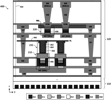
1. An integrated circuit (IC) device, comprising:
a support;
a first thin-film transistor (TFT) in a first layer over the support;
a second TFT in a second layer over the support, wherein the first layer is between the support and the second layer, and each of the first TFT and the second TFT includes a pair of a source electrode and a drain electrode; and
a via having a first end and an opposing second end, wherein the first end is directly electrically connected with a first electrode of the pair of the first TFT and the second end is directly electrically connected with a gate electrode of the second TFT.