| CPC H05K 9/0088 (2013.01) [H04M 1/0277 (2013.01); H05K 1/0203 (2013.01); H05K 9/0024 (2013.01); H05K 9/009 (2013.01)] | 12 Claims |
|
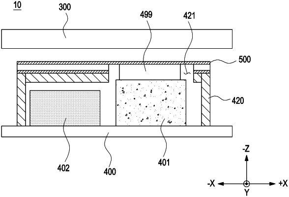
1. An electronic device comprising:
a circuit board;
a first component disposed on the circuit board;
a shield can disposed to surround at least a part of the first component and including an opening; and
a nanofiber film disposed on the shield can to cover the opening,
wherein the nanofiber film includes a first layer, a second layer, and a third layer sequentially laminated in a first direction,
the first layer or the third layer having a lower electrical resistance value than an electrical resistance value of the second layer in a second direction different from the first direction, and
the second layer having a lower electrical resistance value than an electrical resistance value of the first layer or the third layer in the first direction.
|