| CPC H05K 1/0296 (2013.01) [H05K 1/05 (2013.01); H05K 1/09 (2013.01); H05K 3/24 (2013.01); H05K 3/28 (2013.01)] | 6 Claims |
|
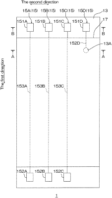
1. A wiring circuit board comprising:
a first insulating layer;
a conductive pattern disposed on the first insulating layer, the conductive pattern having a first terminal, a second terminal, and a wire that electrically connects the first terminal and the second terminal;
a second insulating layer disposed on the first insulating layer and covering the wire without covering at least a part of the first terminal and at least a part of the second terminal; and
a protective layer disposed between the wire and the second insulating layer and protecting the wire,
wherein the protective layer consists of a metal oxide.
|