| CPC H04N 25/705 (2023.01) [H04N 25/77 (2023.01); H04N 25/78 (2023.01)] | 2 Claims |
|
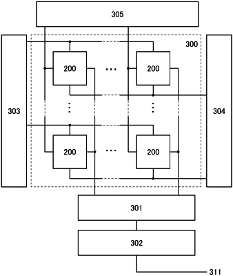
1. An imaging device comprising a pixel,
wherein the pixel comprises a first light-receiving circuit, a second light-receiving circuit, a differential amplifier circuit, and an arithmetic circuit,
wherein the differential amplifier circuit comprises a first transistor, a second transistor, a third transistor, a fourth transistor, and a fifth transistor,
wherein the arithmetic circuit comprises a sixth transistor, a seventh transistor, an eighth transistor, a ninth transistor, a tenth transistor, an eleventh transistor, a first capacitor, and a second capacitor,
wherein first data output from the first light-receiving circuit is input to a gate of the first transistor,
wherein second data output from the second light-receiving circuit is input to a gate of the second transistor,
wherein one of a source and a drain of the first transistor is electrically connected to one of a source and a drain of the fifth transistor,
wherein one of a source and a drain of the second transistor is electrically connected to the one of the source and the drain of the fifth transistor,
wherein the other of the source and the drain of the first transistor is electrically connected to a gate and one of a source and a drain of the third transistor,
wherein the other of the source and the drain of the second transistor is electrically connected to a gate and one of a source and a drain of the fourth transistor,
wherein the gate of the fourth transistor is electrically connected to one of a source and a drain of the sixth transistor,
wherein the other of the source and the drain of the sixth transistor is electrically connected to one electrode of the first capacitor,
wherein the other electrode of the first capacitor is electrically connected to one of a source and a drain of the eighth transistor,
wherein the other of the source and the drain of the eighth transistor is electrically connected to one of a source and a drain of the ninth transistor,
wherein a gate of the eighth transistor is electrically connected to a gate of the ninth transistor,
wherein the other of the source and the drain of the ninth transistor is electrically connected to one electrode of the second capacitor,
wherein the other electrode of the second capacitor is electrically connected to one of a source and a drain of the tenth transistor and a gate of the eleventh transistor, and
wherein the other of the source and the drain of the tenth transistor is electrically connected to the gate of the fourth transistor.
|