| CPC H04L 9/3242 (2013.01) [G06F 3/0622 (2013.01); G06F 3/0659 (2013.01); G06F 3/0673 (2013.01); G06F 11/1068 (2013.01); G06F 11/108 (2013.01); G06F 12/0886 (2013.01); G06F 12/14 (2013.01); G06F 12/1408 (2013.01); G06F 21/78 (2013.01); G06F 21/79 (2013.01); G11C 29/52 (2013.01); H04L 9/0631 (2013.01); H04L 9/0643 (2013.01); H04L 9/0894 (2013.01); G06F 2212/401 (2013.01); G11C 2029/4402 (2013.01); H04L 2209/34 (2013.01)] | 20 Claims |
|
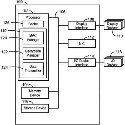
1. An apparatus comprising:
a plurality of cores; and
a memory controller coupled with the plurality of cores, the memory controller to:
decrypt encrypted data to generate decrypted data and decrypt a block correction value in response to a read operation to one or more memory devices, the decrypted data comprising a plurality of data blocks, and the decrypted block correction value comprising a value to repair a data block of the plurality of data blocks;
determine whether the decrypted block correction value matches a result of an XOR operation performed on at least two data blocks of the plurality of data blocks; and
transmit the decrypted data to a cache memory based on a determination that the decrypted block correction value matches the result of the XOR operation performed on the at least two data blocks of the plurality of data blocks.
|