| CPC H04L 7/0079 (2013.01) [G06F 1/08 (2013.01); G09G 5/006 (2013.01); H04L 7/0008 (2013.01); H03K 19/20 (2013.01)] | 20 Claims |
|
1. A receiver circuit comprising:
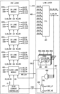
a plurality of data lane modules, each of the plurality of data lane modules configured to receive respective data signals;
a clock lane module configured to receive clock signals and configured to provide each of the plurality of data lane modules with a respective divided clock signal among divided clock signals based on the clock signals;
a bias current controller configured to control a clock bias current provided to the clock lane module; and
a link layer configured to provide a bias control signal to the bias current controller and configured to provide clock gating signals to the clock lane module based on levels of low power data signals output from the plurality of data lane modules and low power clock signals output from the clock lane module, and
wherein the bias current controller, based on the bias control signal, is configured to
cut off the clock bias current in a first power mode,
provide the clock bias current having a first magnitude to the clock lane module in a second power mode, and
provide the clock bias current having a second magnitude greater than the first magnitude to the clock lane module in a third power mode.
|