| CPC H04B 10/2507 (2013.01) [H04B 10/697 (2013.01); H04B 10/801 (2013.01)] | 8 Claims |
|
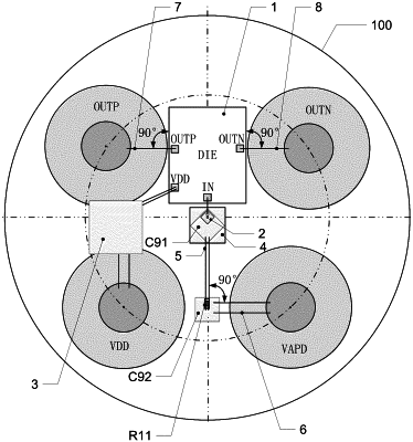
1. A high-speed TIA anti-5G WIFI electromagnetic interference method, comprising:
providing a bare DIE chip (1) of a TIA and an avalanche photodiode APD (2) on a storage platform of a metal tube housing (100), wherein the metal tube housing (100) has a pin GND, a pin VAPD, a pin VDD, a pin OUTP and a pin OUTN;
characterized in that, the method is to stack a high-voltage capacitor C9 and a resistor R11 for constructing a filter circuit on the bare DIE chip of the TIA, wherein the filter circuit filters the ripple of an output pin MIROUT of a current mirror chip CURRENT_MIRROR inside a receiving end ROSA of an optical fiber communication module, and specifically comprises the following steps:
A1: splitting the high-voltage capacitor C9 into two parallel filter capacitors C91 and C92, and satisfy C9=C91+C92, C91=C92;
A2: constructing differential outputs to cancel signal interference by the following steps:
arranging the bare DIE chip (1) of the TIA on a longitudinal axis of the storage platform between the pins OUTP and OUTN;
connecting the pin OUTP to the output pad OUTP on the bare DIE chip (1) of the TIA through a No. 3 gold wire (7) perpendicular to the longitudinal axis;
connecting the pin OUTN to the output pad OUTN on the bare DIE chip (1) of the TIA through a No. 4 gold wire (8) perpendicular to the longitudinal axis;
the No. 3 gold wire (7) and the No. 4 gold wire (8) are of equal length and are kept on the same horizontal level, so as to achieve mutual cancellation of signal interference of differential outputs of the high-speed TIA;
A3: cancel out electromagnetic interference from lens leakage by the following steps:
stacking the avalanche photodiode APD (2), the filter capacitor C91 and a gold-plated pad (4) in sequence on a vertical axis of the bare DIE chip (1) proximal to the TIA, connecting to an input pad IN on the vertical axis of the bare DIE chip (1) of the TIA through a gold wire, and connecting a gold-plated pad (4) to ground through the pin GND;
stacking the resistor R11 and the filter capacitor C92 in sequence on the vertical axis between pins VDD and VAPD, wherein the resistor R11 is connected to the filter capacitor C91 through the No. 1 gold wire (5), the filter capacitor C92 is connected to the pin VAPD through the No. 2 gold wire (6);
the No. 1 gold wire (5) and the No. 2 gold wire (6) form an included angle of 90° to offset the electromagnetic interference leaked from the lens.
|