| CPC H04B 1/40 (2013.01) [H01L 23/49827 (2013.01); H01L 23/66 (2013.01); H01L 24/92 (2013.01); H01L 25/0655 (2013.01); H01L 24/13 (2013.01); H01L 24/16 (2013.01); H01L 24/17 (2013.01); H01L 2223/6616 (2013.01); H01L 2223/6655 (2013.01); H01L 2223/6677 (2013.01); H01L 2224/13025 (2013.01); H01L 2224/131 (2013.01); H01L 2224/13144 (2013.01); H01L 2224/13147 (2013.01); H01L 2224/1329 (2013.01); H01L 2224/133 (2013.01); H01L 2224/16145 (2013.01); H01L 2224/16146 (2013.01); H01L 2224/16227 (2013.01); H01L 2224/17181 (2013.01); H01L 2224/92222 (2013.01); H01L 2924/15311 (2013.01)] | 20 Claims |
|
1. A wireless device comprising:
an antenna configured to transmit and receive a signal;
a transceiver in communication with the antenna; and
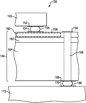
a front-end module including a wafer level chip scale package, the wafer level chip scale package including a semiconductor die that includes an integrated circuit, a first side and a second side, and a plurality of vias, each via configured to provide an electrical connection between the first side and the second side of the semiconductor die, the wafer level chip scale package further including a filter device mounted on the first side of the semiconductor die, the filter device in communication with the integrated circuit, the integrated circuit implemented in a layer on the first side of the semiconductor die and at least some of the vias coupled with the integrated circuit to support an electrical connection between the integrated circuit and mounting features on the second side of the semiconductor die.
|