| CPC H03K 3/017 (2013.01) [H03K 19/20 (2013.01); H04L 25/4902 (2013.01)] | 5 Claims |
|
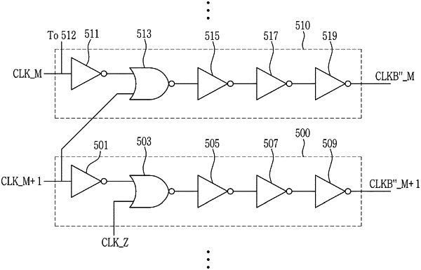
1. A semiconductor device comprising:
a plurality of pulse width modulation circuits,
wherein each of the plurality of pulse width modulation circuits comprises:
a first inverter configured to invert a first clock signal and to output a first inversion signal,
a NOR gate configured to perform a NOR operation on the first inversion signal and a second clock signal and to output a first logic signal according to the NOR operation result,
a second inverter configured to invert the first logic signal and to output a second inversion signal,
a third inverter configured to invert the second inversion signal and to output a third inversion signal, and
a fourth inverter configured to invert the third inversion signal and to output a fourth inversion signal, and
wherein a first one of the plurality of pulse width modulation circuits is configured to receive the first clock signal and the second clock signal,
wherein a second one of the plurality of pulse width modulation circuits is configured to receive the second clock signal, the second clock signal being the first clock signal of the second one of the plurality of pulse width modulation circuits, and
wherein the second clock signal is delayed by a predetermined phase with respect to the first clock signal.
|