US 12,237,831 B2
Network-on-chip (NOC) with flexible data width
Sharath Raghava, Los Gatos, CA (US); Ankireddy Nalamalpu, Portland, OR (US); Dheeraj Subbareddy, Portland, OR (US); Harsha Gupta, Sunnyvale, CA (US); James Ball, San Jose, CA (US); Kavitha Prasad, San Jose, CA (US); and Sean R. Atsatt, Santa Cruz, CA (US)
Assigned to Intel Corporation, Santa Clara, CA (US)
Filed by Intel Corporation, Santa Clara, CA (US)
Filed on May 16, 2023, as Appl. No. 18/198,122.
Application 18/198,122 is a continuation of application No. 17/556,917, filed on Dec. 20, 2021, granted, now 11,700,002.
Application 17/556,917 is a continuation of application No. 17/033,524, filed on Sep. 25, 2020, granted, now 11,342,918, issued on May 24, 2022.
Application 17/033,524 is a continuation of application No. 16/234,212, filed on Dec. 27, 2018, granted, now 10,790,827, issued on Sep. 29, 2020.
Prior Publication US 2023/0370068 A1, Nov. 16, 2023
Int. Cl. H03K 19/177 (2020.01); H03K 19/17736 (2020.01); H03K 19/17796 (2020.01); H04L 41/5019 (2022.01); H04L 41/5003 (2022.01)
CPC H03K 19/17736 (2013.01) [H03K 19/17796 (2013.01); H04L 41/5019 (2013.01); H04L 41/5003 (2013.01)] 16 Claims
OG exemplary drawing
 
1. A multi-die system, comprising:
a processing circuit disposed on a first die; and
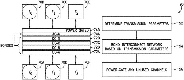
a network-on-chip disposed at least in part on the first die, wherein the network-on-chip is configurable to facilitate memory transactions between the first die and a second die, wherein the network-on-chip comprises a plurality of data lanes, wherein the network-on-chip is configurable to transmit data between the first die and the second die via a bus formed from the plurality of data lanes, and wherein the network-on-chip is configurable to reduce power consumed at least in part by reducing a width of the bus based on traffic latency and bandwidth.