| CPC H03H 9/0576 (2013.01) [H03H 9/0561 (2013.01); H03H 9/725 (2013.01); H03H 9/74 (2013.01); H03H 2001/0085 (2013.01)] | 10 Claims |
|
1. A filter device comprising:
a multilayer panel with wiring;
a piezoelectric substrate mounted to the multilayer panel;
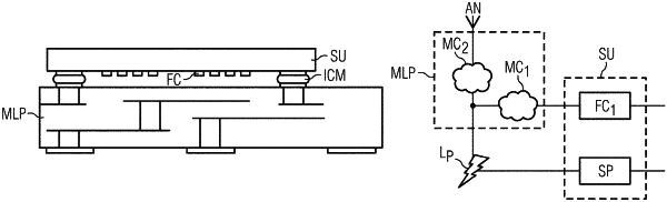
a first filter circuit;
a signal path comprising a second filter circuit, wherein the first filter circuit and the second filter circuit are both filter circuits being realized on a top surface of the piezoelectric substrate and connected to a common antenna terminal on the piezoelectric substrate;
a first matching circuit having a first end connected to the common antenna terminal on the piezoelectric substrate and a second end connected to the signal path with the second filter circuit, the first matching circuit including the wiring in the multilayer panel; and
a common node to which the first filter circuit, the signal path and the common antenna terminal are connected to, the common node being a pad located on the top surface of the piezoelectric substrate.
|