| CPC H03F 3/245 (2013.01) [H03F 1/56 (2013.01); H03F 1/565 (2013.01); H03F 3/195 (2013.01); H04B 1/0458 (2013.01); H03F 2200/387 (2013.01); H03F 2200/451 (2013.01)] | 20 Claims |
|
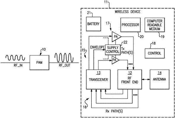
1. An impedance adjustment circuit comprising:
an input node configured to receive a radio frequency signal from a power amplifier located on a power amplifier die;
an output node configured to provide the radio frequency signal to an antenna switch located on an antenna switch die;
a plurality of electrical components arranged between the input node and the output node, a first electrical component of the plurality of electrical components located between the power amplifier die and the antenna switch die and a second electrical component of the plurality of electrical components located on the antenna switch die; and
at least one switch configured to selectively electrically connect at least one of the first electrical component and the second electrical component to the input node and the output node to adjust an impedance of the power amplifier, the impedance of the power amplifier is adjusted from a natural tune point in a direction towards a target tuned impedance point when viewed on a Smith chart for each state of the at least one switch.
|