| CPC H02M 1/08 (2013.01) [H02M 7/003 (2013.01); H02M 7/537 (2013.01); H05K 1/0298 (2013.01); H05K 1/181 (2013.01); H05K 3/32 (2013.01); H05K 2201/09227 (2013.01); H05K 2201/10015 (2013.01); H05K 2201/10166 (2013.01); H05K 2201/10522 (2013.01)] | 23 Claims |
|
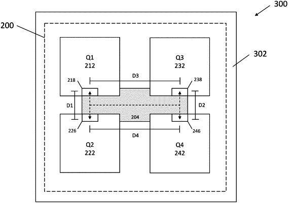
1. A power switching circuit comprising:
a switching node;
a first transistor, a second transistor, a third transistor, and a fourth transistor, the first transistor and the third transistor each having a first connection coupled to the switching node, and the second transistor and the fourth transistor each having a second connection coupled to the switching node;
a first conduction path from the first connection of the first transistor, through the switching node, to the second connection of the fourth transistor, the first conduction path having a first length; and
a second conduction path from the first connection of the first transistor, through the switching node, to the second connection of the second transistor, the second conduction path having a second length,
wherein the first length of the first conduction path is greater than the second length of the second conduction path.
|