| CPC H01S 5/1003 (2013.01) [H01S 5/021 (2013.01); H01S 5/22 (2013.01); H01S 5/3013 (2013.01)] | 11 Claims |
|
1. A method of manufacturing a semiconductor optical device, comprising:
a step of bonding a semiconductor element to a substrate that includes silicon, the semiconductor element being made of a III-V compound semiconductor and having optical gain;
after the step of bonding the semiconductor element, a step of molding the semiconductor element by wet-etching; and
after the step of molding the semiconductor element, a step of forming a mesa at the semiconductor element,
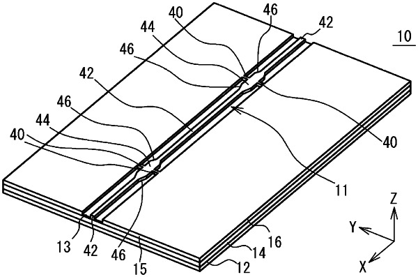
wherein the substrate includes a waveguide, a groove that extends along the waveguide, a terrace that is positioned on a side of the groove opposite to the waveguide, and a wall that covers the groove and the wall has a wall upper surface,
wherein the waveguide includes a first portion and a second portion, the first portion has a first portion upper surface and the second portion has a second portion upper surface,
wherein the wall upper surface, the first portion upper surface, and the second portion upper surface are each positioned at a same height from a bottom surface of the groove, and
wherein the step of bonding the semiconductor element is a step of bonding the semiconductor element to the waveguide, the groove, the terrace, and the wall of the substrate.
|