| CPC H01Q 9/0414 (2013.01) [H01Q 1/2283 (2013.01); H05K 1/0243 (2013.01); H05K 1/025 (2013.01); H05K 1/115 (2013.01); H05K 2201/0969 (2013.01); H05K 2201/10098 (2013.01)] | 17 Claims |
|
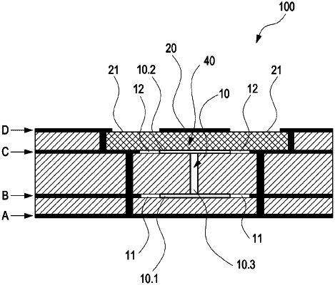
1. Printed circuit board-integrated antenna configured to transmit/receive data, the antenna being formed on adjacent layers of said printed circuit board, the adjacent layers being interconnected by a plurality of vias to form a conductive solid area, wherein said adjacent layers of the printed circuit board comprise a lower layer, a lower middle layer, an upper middle layer, and an upper layer, the antenna comprising:
an intermediate section comprising first and second patch elements interconnected by at least one via, wherein the first patch element is disposed in the lower middle layer and separated by a gap from the conductive solid area, the second patch element is disposed in the upper middle layer and separated by a gap from the conductive solid area;
a parasitic patch element disposed in the upper layer and separated by a gap from the conductive solid area; and
a strip line connected directly to an edge of the first patch element, the strip line being disposed in the lower middle layer configured to communicate a data signal to or from the intermediate section when transmitting/receiving data.
|