US 12,237,589 B2
Wireless communication technology, apparatuses, and methods
Erkan Alpman, Portland, OR (US); Arnaud Lucres Amadjikpe, Beaverton, OR (US); Omer Asaf, Oranit (IL); Kameran Azadet, San Ramon, CA (US); Rotem Banin, Even-Yehuda (IL); Miroslav Baryakh, Petach Tikva (IL); Anat Bazov, Petach-Tikva (IL); Stefano Brenna, Hillsboro, OR (US); Bryan K. Casper, Portland, OR (US); Anandaroop Chakrabarti, Beaverton, OR (US); Gregory Chance, Chandler, AZ (US); Debabani Choudhury, Thousand Oaks, CA (US); Emanuel Cohen, Zichron Yaacov (IL); Claudio Da Silva, Portland, OR (US); Sidharth Dalmia, Fair Oaks, CA (US); Saeid Daneshgar Asl, Portland, OR (US); Kaushik Dasgupta, Hillsboro, OR (US); Kunal Datta, Los Angeles, CA (US); Brandon Davis, Phoenix, AZ (US); Ofir Degani, Haifa (IL); Amr M. Fahim, Portland, OR (US); Amit Freiman, Haifa (IL); Michael Genossar, Modiin (IL); Eran Gerson, Pardes Hana (IL); Eyal Goldberger, Moshav Beherotaim (IL); Eshel Gordon, Aloney Aba (IL); Meir Gordon, Holon (IL); Josef Hagn, Neubiberg (DE); Shinwon Kang, San Francisco, CA (US); Te Yu Kao, San Jose, CA (US); Noam Kogan, Tel-Aviv (IL); Mikko S. Komulainen, Oulu (FI); Igal Yehuda Kushnir, Hod-Hasharon (IL); Saku Lahti, Tampere (FI); Mikko M. Lampinen, Nokia (FI); Naftali Landsberg, Ramat Gan (IL); Wook Bong Lee, San Jose, CA (US); Run Levinger, Tel Aviv (IL); Albert Molina, Alcobendas (ES); Resti Montoya Moreno, Helsinki (FI); Tawfiq Musah, Hillsboro, OR (US); Nathan G. Narevsky, Portland, OR (US); Hosein Nikopour, San Jose, CA (US); Oner Orhan, San Jose, CA (US); Georgios Palaskas, Portland, OR (US); Stefano Pellerano, Beaverton, OR (US); Ron Pongratz, Tel Aviv (IL); Ashoke Ravi, Portland, OR (US); Shmuel Ravid, Haifa (IL); Peter Andrew Sagazio, Portland, OR (US); Eren Sasoglu, Mountain View, CA (US); Lior Shakedd, Kfar Bilu (IL); Gadi Shor, Tel Aviv (IL); Baljit Singh, San Jose, CA (US); Menashe Soffer, Katzir (IL); Ra'anan Sover, Haifa (IL); Shilpa Talwar, Cupertino, CA (US); Nebil Tanzi, Hoffman Estates, IL (US); Moshe Teplitsky, Tel-Aviv (IL); Chintan S. Thakkar, Portland, OR (US); Jayprakash Thakur, Bangalore (IN); Avi Tsarfati, Rishon le Zion (IL); Yossi Tsfati, Rishon le Zion (IL); Marian Verhelst, Portland, OR (US); Nir Weisman, Hod Hasharon (IL); Shuhei Yamada, Hillsboro, OR (US); Ana M. Yepes, Portland, OR (US); and Duncan Kitchin, Beaverton, OR (US)
Assigned to Intel Corporation, Santa Clara, CA (US)
Filed by Intel Corporation, Santa Clara, CA (US)
Filed on May 2, 2022, as Appl. No. 17/734,529.
Application 17/734,529 is a division of application No. 16/472,830, granted, now 11,424,539, previously published as PCT/US2017/067739, filed on Dec. 20, 2017.
Claims priority of provisional application 62/570,680, filed on Oct. 11, 2017.
Claims priority of provisional application 62/527,818, filed on Jun. 30, 2017.
Claims priority of provisional application 62/511,398, filed on May 26, 2017.
Claims priority of provisional application 62/437,385, filed on Dec. 21, 2016.
Prior Publication US 2022/0384956 A1, Dec. 1, 2022
Int. Cl. H01Q 5/47 (2015.01); H01Q 1/24 (2006.01); H01Q 1/38 (2006.01); H01Q 1/48 (2006.01); H01Q 3/24 (2006.01); H01Q 9/04 (2006.01); H01Q 21/24 (2006.01); H03L 7/14 (2006.01); H04B 1/3827 (2015.01); H04B 7/0456 (2017.01); H04B 7/06 (2006.01); H04B 15/04 (2006.01)
CPC H01Q 9/0414 (2013.01) [H01Q 1/243 (2013.01); H01Q 1/38 (2013.01); H01Q 1/48 (2013.01); H01Q 3/24 (2013.01); H01Q 5/47 (2015.01); H01Q 21/24 (2013.01); H03L 7/145 (2013.01); H04B 1/3827 (2013.01); H04B 7/0482 (2013.01); H04B 7/0639 (2013.01); H04B 15/04 (2013.01)] 20 Claims
OG exemplary drawing
 
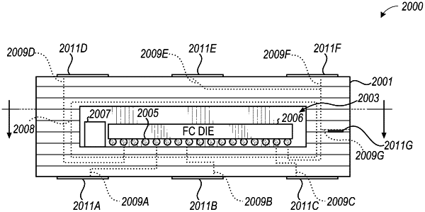
1. A low-loss radio subsystem, comprising:
at least one silicon die configured to include electronic circuits operable to generate electronic signals for operation of a predetermined number of antennas;
a laminar substrate comprising a plurality of parallel layers, wherein the at least one silicon die is embedded between a first layer and a second layer of the plurality of parallel layers of the laminar substrate;
the predetermined number of antennas comprising at least a first antenna configured on or within the first layer and at least a second antenna configured on or within the second layer of the laminar substrate; and
a conductive signal feed structure connected between the at least one silicon die and the predetermined number of antennas and configured to feed the electronic signals to the predetermined number of antennas.