| CPC H01M 8/1213 (2013.01) [H01M 8/1226 (2013.01); H01M 8/2475 (2013.01)] | 17 Claims |
|
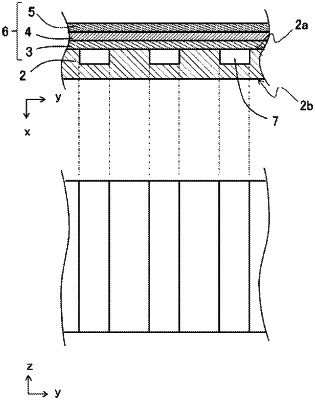
1. A cell comprising:
a metal plate comprising a first surface, and a second surface that faces the first surface, the metal plate containing Cr;
an element portion disposed on the first surface, the element portion comprising a first electrode layer, a solid electrolyte layer located on and in direct contact with the first electrode layer, and a second electrode layer located on the solid electrolyte layer; and
a first intermediate layer located between the first surface and the first electrode layer, wherein
the first intermediate layer contains Cr2O3 and a first conductive particle different from Cr2O3.
|