| CPC H01L 33/62 (2013.01) [H01L 33/52 (2013.01); H01L 2933/005 (2013.01); H01L 2933/0066 (2013.01)] | 17 Claims |
|
1. A light emitting diode (LED) package comprising:
a substrate having an upper surface, and a lower surface opposite to said upper surface;
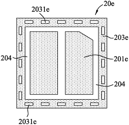
a metal stage formed on said upper surface of said substrate;
at least one LED chip mounted on said metal stage; and
a packaging material covering said LED chip, said metal stage and said substrate, said packaging material and said metal stage being engaged with each other;
wherein said metal stage includes a chip-mounting region for mounting said LED chip thereon, and a boundary region;
wherein said boundary region is located at a periphery of said metal stage;
wherein said boundary region includes a boundary section that is spaced apart from said chip-mounting region;
wherein electric connection between said boundary section and said chip-mounting region is not established so that said boundary section is electrically insulated from said LED chip; and
wherein said boundary section has an enclosed structure continuously surrounding said chip-mounting region, said boundary section having one of a through hole and a comb structure.
|