| CPC H01L 33/382 (2013.01) [H01L 33/46 (2013.01); H01L 33/62 (2013.01)] | 20 Claims |
|
1. A UV light emitting device, comprising:
a mount substrate including electrode pads;
a light source disposed on the mount substrate, wherein the light source includes:
an n-type semiconductor layer;
a mesa disposed on the n-type semiconductor layer, and including a well layer configured to emit light having an ultraviolet wavelength and a p-type semiconductor layer;
an n-ohmic contact layer in contact with the n-type semiconductor layer;
a p-ohmic contact layer in contact with the p-type semiconductor layer;
an n-bump electrically connected to the n-ohmic contact layer; and
a p-bump electrically connected to the p-ohmic contact layer,
wherein:
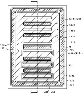
the mesa has a rectangular shape and includes a plurality of vias exposing the n-type semiconductor layer,
the plurality of vias are arranged in parallel to one another,
the n-type semiconductor layer includes a region having a higher band gap than a band gap of the well layer configured to emit light having the ultraviolet wavelength, and
the n-ohmic contact layer includes a plurality of contact regions spaced apart from each other by the mesa.
|