| CPC H01L 31/1804 (2013.01) [C30B 29/06 (2013.01); C30B 31/08 (2013.01); C30B 31/185 (2013.01); C30B 33/02 (2013.01); H01L 21/22 (2013.01); H01L 21/324 (2013.01); H01L 31/0288 (2013.01); H01L 31/068 (2013.01); H01L 31/1864 (2013.01); Y02E 10/547 (2013.01); Y02P 70/50 (2015.11)] | 1 Claim |
|
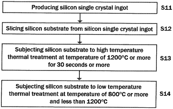
1. A method for manufacturing a solar cell, comprising:
preparing a Czochralski silicon single crystal ingot doped with a p-type dopant or an n-type dopant and containing oxygen atoms of at least 12 ppm;
preparing a silicon substrate from the Czochralski silicon single crystal ingot;
subjecting the silicon substrate to low temperature thermal treatment at a temperature of 800° C. or more and less than 1200° C. so as to fabricate a solar cell,
wherein either the Czochralski silicon single crystal ingot, or the silicon substrate, is subjected to, before the low temperature thermal treatment, high temperature thermal treatment at a temperature of more than 1200° C. for 5 minutes or more and 30 minutes or less, so that oxide precipitate nuclei are dissolved and a homogenous solid solution of oxide precipitate nuclei is formed throughout the silicon substrate;
subjecting the silicon substrate to texture etching before the high temperature thermal treatment; and
subjecting the fabricated solar cell to an electroluminescence image test to check that spiral oxygen-induced defect patterns are not observed;
wherein the conversion efficiency of the solar cell in which the spiral oxygen-induced defect patterns are not observed in the electroluminescence image test is about 20% and the variation thereof is about 0.1%.
|